Understanding PLONK (Part 1): Plonkish Arithmetization
Arithmetization refers to transforming computations into mathematical objects and then performing zero-knowledge proofs. Plonkish arithmetization is a specific arithmetization method in the Plonk proof system. Prior to the introduction of Plonkish, the mainstream circuit representation was R1CS, widely used in systems such as Pinocchio, Groth16, and Bulletproofs. In 2019, the Plonk scheme proposed a seemingly retrograde circuit encoding method. However, due to its extreme application of polynomial encoding, Plonk is no longer limited to “addition gates” and “multiplication gates” in arithmetic circuits, but can support more flexible “custom gates” and “lookup gates”.
Let’s first review the circuit encoding of R1CS, which is the most commonly used arithmetic scheme. Then we will compare it with the introduction of Plonkish encoding.
Arithmetic circuits and arithmeticization of R1CS
An arithmetic circuit consists of several multiplication gates and addition gates. Each gate has “two input” pins and one “output” pin, and any output pin can be connected to multiple input pins of gates.
First, let’s look at a very simple arithmetic circuit:
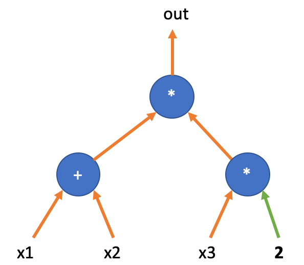
This circuit represents such a calculation:
There are 4 variables in the circuit, with three variables being input variables , one output variable , and one constant input with a value of .
A circuit has two states: “blank state” and “operational state”. When the input variables do not have specific values, the circuit is in the “blank state”, and we can only describe the relationship between the circuit wires, or the structural topology of the circuit.
The next step is to encode the “blank state” of the circuit, which means encoding the positions of each gate and their interconnecting wire relationships.
R1CS is centered around multiplication gates in the graph, using three “selector” matrices to connect the “left input,” “right input,” and “output” of the multiplication gates to respective variables.
Let’s start by looking at the left input of the multiplication gate at the top of the diagram. It can be described using the table below:
\begin{array}{|c|c|c|c|c|} \hline 1 & x_1 & x_2 & x_3 & out \ \hline 0 & 1 & 1 & 0 & 0 \ \hline \end{array}
This form has only one row, so we can use a vector to represent that the left input of the multiplication gate is connected to two variables, and . Remember, all addition gates will be expanded into sums (or linear combinations) of multiple variables.
再看看其右输入,连接了一个变量 和一个常数值,等价于连接了 的两倍,那么右输入的选择子矩阵可以记为
\begin{array}{|c|c|c|c|c|} \hline 1 & x_1 & x_2 & x_3 & out \ \hline 0 & 0 & 0 & 2 & 0 \ \hline \end{array}
Here, it can also be represented by a row vector , where the represents the constant terminal of the circuit in the above diagram.
The output of the final multiplication gate can be described as , with the output variable being .
\begin{array}{|c|c|c|c|c|} \hline 1 & x_1 & x_2 & x_3 & out \ \hline 0 & 0 & 0 & 0 & 1 \ \hline \end{array}
With three vectors (U, V, W), we can constrain the operation of the circuit through an “inner product” equation:
After simplifying this equation, we can obtain:
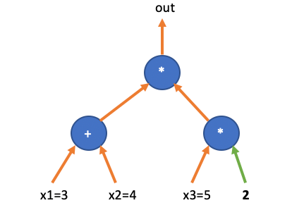
If we substitute these variables with the assignment vector , then the circuit operation can be verified through the “inner product” equation:
And if we have an incorrectly assigned vector, such as , it does not satisfy the “inner product equation”:
The result of the left-side arithmetic is , and the result of the right-side arithmetic is . Of course, we can verify that is also a valid (satisfying circuit constraints) assignment.
Not every circuit has an assignment vector. Circuits that have a valid assignment vector are called satisfiable circuits. Determining whether a circuit is satisfiable is an NP-Complete problem and also an NP-hard problem.
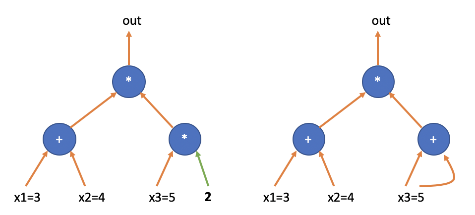
The two multiplication gates in the examples are not the same. The multiplication gate above has variables in both inputs, while the multiplication gate below has a variable on one side and a constant on the other side. For the latter type of “constant multiplication gate”, we also consider them as special “addition gates”. As shown in the diagram below, the multiplication gate in the bottom right of the left circuit is equivalent to the addition gate in the bottom right of the right circuit.
So if a circuit contains more than two multiplication gates, we cannot use the inner product relationship between the vectors to represent the operation, and we need to construct an operation relationship between “three matrices”.
Multiple multiplication gates
For example, in the circuit shown below, there are two multiplication gates, and both their left and right inputs involve variables.
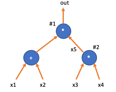
This circuit represents such a calculation:
We encode the circuit based on the multiplication gates. In the first step, the multiplication gates in the circuit are numbered sequentially (the order of numbering doesn’t matter as long as it is consistent). The two multiplication gates in the diagram are encoded as #1 and #2.
And then we need to give variable names to the intermediate wires of each multiplication gate: for example, four input variables are denoted as , with being the output of the second multiplication gate and also serving as the right input of the first multiplication gate. And is the output of the first multiplication gate. Therefore, we can obtain a vector of variable names:
The “blank state” of this circuit can be encoded using the following three matrices:
I understand. Here is the text:
Where is the number of multiplication gates, and is approximately the number of wires. Each row of the matrix “selects” the input/output variables of the corresponding multiplication gate. For example, we define the left input matrix of the circuit:
\begin{array}{|c|c|c|c|c|} \hline x_1 & x_2 & x_3 & x_4 & x_5 & out & \texttt{i} \ \hline 1 & 1 & 0 & 0 & 0 & 0 & \texttt{1}\ \hline 0 & 0 & 1 & 0 & 0 & 0 & \texttt{2}\ \hline \end{array}
The left input of the first multiplier gate is , and the left input of the second multiplier gate is . The right input matrix is defined as:
\begin{array}{|c|c|c|c|c|} \hline x_1 & x_2 & x_3 & x_4 & x_5 & out &\texttt{i}\ \hline 0 & 0 & 0 & 0 & 1 & 0 & \texttt{1}\ \hline 0 & 0 & 0 & 1 & 0 & 0 & \texttt{2}\ \hline \end{array}
The right input of gate No. 1 is , and the right input of the second multiplication gate is . Finally, the output matrix is defined as follows:
\begin{array}{|c|c|c|c|c|} \hline x_1 & x_2 & x_3 & x_4 & x_5 & out & \texttt{i}\ \hline 0 & 0 & 0 & 0 & 0 & 1 & \texttt{1}\ \hline 0 & 0 & 0 & 0 & 1 & 0 & \texttt{2}\ \hline \end{array}
We treat all the wire assignments as a vector: (here using the letter , taken from the first letter of Assignments)
In the above example, the “assignment vector” is
So we can easily verify the following equation.
The symbol represents Hadamard Product, which indicates “element-wise multiplication”. Expanding the above element-wise multiplication equation, we can obtain the operation process of this circuit:
\left[ \begin{array}{c} x_1 + x_2 \ x_3 \ \end{array} \right] \circ \left[ \begin{array}{c} x_5 \ x_4 \ \end{array} \right]= \left[ \begin{array}{c} out \ x_5 \ \end{array} \right]
Please note that in general, a “assignment vector” needs a variable with a fixed value of , which is necessary to handle constant inputs in addition gates.
Advantages and disadvantages
Due to the R1CS encoding being centered around multiplication gates, the addition gates in the circuit do not increase the number of rows in the matrices , thus having little impact on the performance of the Prover. The encoding of R1CS circuits is clear and simple, which facilitates the construction of various SNARK schemes on top of it.
The encoding scheme in the 2019 Plonk paper requires encoding both addition and multiplication gates, which seems to increase the number of constraints and decrease the proving performance. However, the Plonk team subsequently introduced additional gates besides multiplication and addition, such as gates for range checks and XOR operations. Moreover, Plonk supports any gate with polynomial relations between its inputs and outputs, known as Custom Gates, as well as state transition gates for implementing RAM. With the introduction of lookup gates, the Plonk scheme gradually became the preferred choice for many applications, and its encoding method also gained a dedicated term: Plonkish.
Plonkish Arithmetic Door
Looking back at the example circuit, we will number all three gates as , and we will also mark the output value of the adder gate as variable .
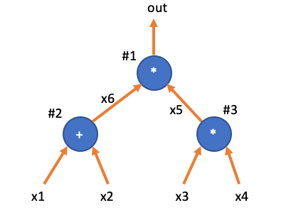
Clearly, the above circuit satisfies three constraints:
-
-
-
I understand. Here is the translation:
“”
We define a matrix to represent the constraints (where is the number of arithmetic gates):
\begin{array}{c|c|c|c|} \texttt{i} & w_a & w_b & w_c \ \hline \texttt{1} & x_6 & x_5 & out \ \texttt{2} & x_1 & x_2 & x_6 \ \texttt{3} & x_3 & x_4 & x_5 \ \end{array}
In order to differentiate addition and multiplication, we define a vector to represent the operator.
\begin{array}{c|c|c|c|} \texttt{i} & q_L & q_R & q_M & q_C & q_O \ \hline \texttt{1} & 0 & 0 & 1 & 0& 1 \ \texttt{2} & 1 & 1 & 0 & 0& 1 \ \texttt{3} & 0 & 0 & 1 & 0& 1 \ \end{array}
So we can represent the three constraints using the following equations:
If we substitute and expand the equation above, we can obtain the following constraint equations:
\left[ \begin{array}{c} 0\ 1 \ 0\ \end{array} \right] \circ \left[ \begin{array}{c} x_6 \ x_1 \ x_5\ \end{array} \right] + \left[ \begin{array}{c} 0\ 1 \ 0\ \end{array} \right] \circ \left[ \begin{array}{c} x_5 \ x_2 \ x_4\ \end{array} \right] + \left[ \begin{array}{c} 1\ 0 \ 1\ \end{array} \right] \circ \left[ \begin{array}{c} x_6\cdot x_5 \ x_1\cdot x_2 \ x_3\cdot x_4\ \end{array} \right]=\left[ \begin{array}{c} 1\ 1 \ 1\ \end{array} \right] \circ \left[ \begin{array}{c} out \ x_6 \ x_5\ \end{array} \right]
Simplified to:
\left[ \begin{array}{c} 0 \ x_1 \ 0\ \end{array} \right] + \left[ \begin{array}{c} 0 \ x_2 \ 0\ \end{array} \right] + \left[ \begin{array}{c} x_6\cdot x_5 \ 0 \ x_3\cdot x_4\ \end{array} \right]=\left[ \begin{array}{c} out \ x_6 \ x_5\ \end{array} \right]
This is exactly the calculation constraint of three arithmetic operations.
In summary, Plonkish requires a matrix to describe the circuit’s blank state, while all assignments are written into the matrix . For the exchange protocol between the Prover and Verifier, is the Prover’s witness, which is considered secret and kept confidential from the Verifier. The matrix represents a circuit description that achieves consensus between both parties.
However, having only the matrix is not sufficient to accurately describe the circuit in the example above.
Copy Constraints
Compare the following two circuits. Their Q matrices are completely identical, but they are completely different.
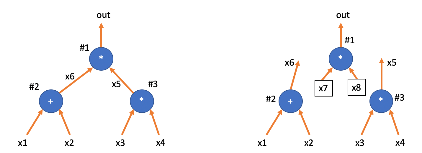
The difference between the two circuits lies in whether are connected to gate #1. If the Prover directly fills in the assignment of the circuit in the table, an “honest” Prover would fill in the same value in the positions and ; while a “malicious” Prover could fill in different values. If the malicious Prover also fills in different values in and , then in reality, the Prover is proving the circuit on the right side of the diagram, not the agreed-upon circuit between the Verifier and the Prover (on the left side).
\begin{array}{c|c|c|c|} i & w_a & w_b & w_c \ \hline 1 & \boxed{x_6} & \underline{x_5} & out \ 2 & x_1 & x_2 & \boxed{x_6} \ 3 & x_3 & x_4 & \underline{x_5} \ \end{array}
We need to add new constraints that require in the right circuit diagram and . This is equivalent to demanding that when Prover fills in multiple positions in the table with the same variable, they must fill in equal values.
This requires a new type of constraint called “Copy Constraint”. Plonk uses “Permutation Proofs” to ensure that the values at multiple positions in the table satisfy the copy relationship. We continue to use the example of the circuit diagram above to illustrate its basic idea:
Imagine that we arrange all the position indices in table into a vector:
Then swap the two positions that should be equal, for example, in the figure above, it is required that and . Thus, we obtain the following positional vectors:
Then we ask the Prover to prove that: table remains the same after the permutation above. The equality before and after the permutation ensures that the Prover cannot cheat.
Here’s another example, when constraining that three (or more) values in a vector must be equal, you only need to shift the values at these three (or more) positions cyclically (left or right), and then prove that the shifted vector is equal to the original vector. For example:
If we want to prove that , then we only need to prove:
In the vector after shuffling, are moved and swapped to the right in sequence, meaning is placed in the original position of , while is placed in the position of , and is placed in the position of .
If , then all the values at the corresponding positions of and should be equal. It can be deduced that: , , , which means . This method is applicable to any number of equivalent relationships. (For the subsequent method of proving the equality of two vectors, please refer to the next chapter.)
So how to describe the exchange in the circuit assignment table? We only need to record the vector, of course, the vector can also be written in the form of a table:
\begin{array}{c|c|c|c|} i & \sigma_a & \sigma_b & \sigma_c \ \hline 1 & \boxed{w_{c,2}} & \underline{w_{c,3}}& w_{c,1} \ 2 & w_{a,2} & w_{b,2} & \boxed{w_{a,1}} \ 3 & w_{a,3} & w_{b,3} & \underline{w_{b,1}} \ \end{array}
Adding , the blank circuit can be described as , where the assignment of the circuit is .
Comparison again
The width of the table in R1CS depends on the number of wires, and the number of rows depends on the number of multiplication gates. This construction treats arithmetic circuits as consisting only of multiplication gates, but each gate has multiple input pins (up to the total number of wires). On the other hand, Plonkish treats addition and multiplication gates equally, and because there are only two input pins, the width of the table is fixed at three columns (although the table can be expanded to support more advanced gates). This feature allows Plonk to utilize the Permutation Argument for the implementation of copy constraints.
…, and thus our linear contraints are just wiring constraints that can be reduced to a permutation check.
按照 Plonk 论文的统计,一般情况下,算术电路中加法门的数量是乘法门的两倍。如果这样看来, 表格的行数会三倍于 R1CS 的矩阵。但这个让步会带来更多的算术化灵活度。
Circuit verification protocol framework
With the description and assignment of the circuit blank structure, we can roughly describe the protocol framework of Plonk.
First, the Prover and Verifier agree on a common circuit, . Assuming the public output of the circuit is , and are the secret inputs.
Fill in the matrix (Invisible to Verifier):
\begin{array}{c|c|c|c|} i & w_a & w_b & w_c \ \hline 1 & \boxed{x_6} & \underline{x_5} & [out] \ 2 & x_1 & x_2 & \boxed{x_6} \ 3 & x_3 & x_4 & \underline{x_5} \ 4 & 0 & 0 & [out] \ \end{array}
The additional fourth line is added to introduce an extra arithmetic constraint: , where the value of is explicitly shown in the matrix .
The corresponding matrix for the consensus of Prover and Verifier is
\begin{array}{c|c|c|c|} i & q_L & q_R & q_M & q_C & q_O \ \hline 1 & 0 & 0 & 1 & 0& 1 \ 2 & 1 & 1 & 0 & 0& 1 \ 3 & 0 & 0 & 1 & 0& 1 \ 4 & 0 & 0 & 0 & 99& 1 \ \end{array}
I understand. Here is the text:
“In the fourth line constraint, it ensures that . By substituting into the arithmetic constraint below, we obtain , which means w_c99\sigmaoutw_{c,1}w_{c,4} \begin{array}{c|c|c|c|} i & \sigma_a & \sigma_b & \sigma_c \ \hline 1 & \boxed{w_{c,2}} & \underline{w_{c,3}} & [w_{c,4}] \ 2 & w_{a,2} & w_{b,2} & \boxed{w_{a,1}} \ 3 & w_{a,3} & w_{b,3} & \underline{w_{b,1}} \ 4 & w_{a,4} & w_{b,4} & [w_{c,1}]\ \end{array} i\in(1,2,3,4)WW(\sigma_a(X),\sigma_b(X),\sigma_c(X))(w_a(X),w_b(X),w_c(X))$. Also, how does the Verifier verify the circuit operations through polynomials, please refer to the following chapters.
References
-
I understand. Here is the translation:
[BG12] Bayer, Stephanie, and Jens Groth. “Efficient zero-knowledge argument for correctness of a shuffle.” Annual International Conference on the Theory and Applications of Cryptographic Techniques. Springer, Berlin, Heidelberg, 2012.
-
I understand. Here is the text:
[GWC19] Ariel Gabizon, Zachary J. Williamson, and Oana Ciobotaru. “Plonk: Permutations over lagrange-bases for oecumenical noninteractive arguments of knowledge.” Cryptology ePrint Archive (2019).